Training and Plasma School - plasway-Technologies GmbH
Way´s to efficiency
Maecenas vitae congue augue,
nec volutpat risus.
Hauptmenü:
One Day Training Classes in
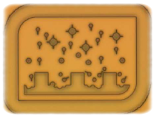
Atomic Layer Processing (ALE, PEALD)
Typical Topics:
Basics principles of Atomic Layer Processing (ALP)
Basics principles of Atomic Layer Processing (ALP)
Applications of ALD & ALE
(PE)ALD & ALE Equipment and Design
(PE)ALD & ALE Precusrors & Gases
In-situ Process characterisation
Market overview &
Forecast 2015-2020
The topics can be set up individualy on request.
Two Day Training Classes
in Plasma Etching and PECVD
in Plasma Etching and PECVD
Typical Topics:
- Reactive Gas Glow Discharges: Plasma etching, reactive ion etching, and PECVD
- Operation of Low and High Density Plasma Sources
- Influence of major Hardware Items (ESC,..)
- Surface Science Aspects of Plasma Etching
- The Role of Energetic Ion Bombardment in Obtaining Etch Profile Anisotropy
- Etching of Silicon and Its Compounds in Halogen-based Etching
- PECVD and It´s Role in Plasma Etching
- PECVD Processes of Greatest Importance in Semiconductor Manufacturing
The topics can be set up individualy on request.